Intro
This write-up is meant to document a recent test of the ADS7865, a stand-alone analog to digital converter (ADC) IC. The ADC a fundamental component within this acoustics system. While the AM3359 processor inside the beaglebone has a built-in ADC. It’s limited to 200k samples per second. This might get knocked down to something like 50k samples per second when working with 4 active channels. This is rather slow for the application at hand, which is a time delay measurement of a 22kHz signal on 4 channels. With a standalone ADC like the ADS7865, this acoustics system should be able sample at 2MHz throughput. The ADS7865 also has the added bonus of dual track and hold amplifiers and an architecture that allows simultaneous sampling at 2 channels at a time. Given this, the ADC should be able to sample 4 channels at a rate of 1MHz per channel, which is more than enough for this application.
Early Hardware test
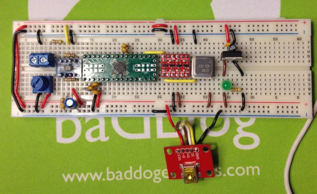
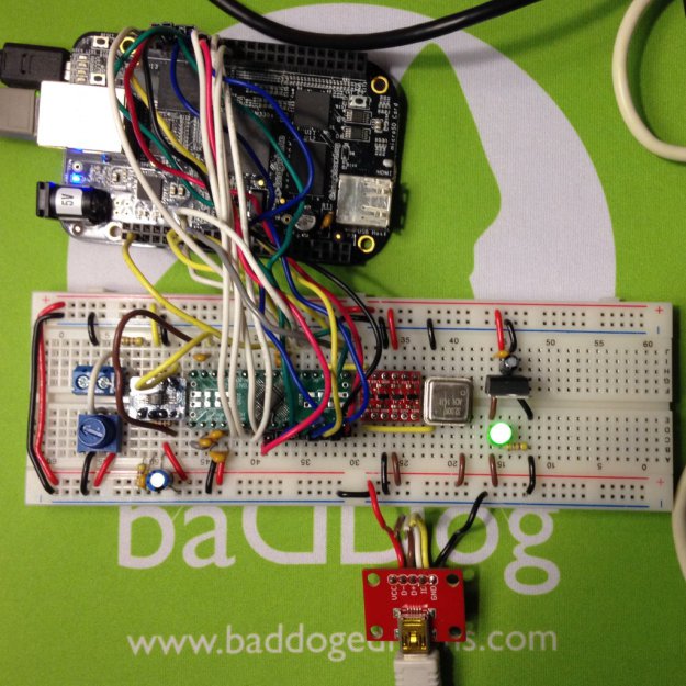
This test board consists of the ADS7865 ADC, THS4531 differential amplifier, 32 Mhz Ocillator (connected to a bidirectional level shifter), 3.3V regulators, 10k pot for driving a signal through the differential amplifier, and a USB connection for power.
Early tests of the THS4531 differential amplifier show that it rails out 110mV from the positive supply. The spec sheet says it should also rail out 60mV from the bottom supply. Thus, with a 3.3V voltage range, the differential output has a voltage range of ~6.26V from Vop to Von. I also obtained an LME49724 differential amplifier and attempted to test it in the same manner, but it turns out that this chip will not work on a 0V – 3.3V supply. It needs at least a 5V supply. This chip will have to be tested at a later time.
Early Software trials
I tried making a Python library to control the GPIO pins. At first, it was awesome, because using the python to control SysFS was pretty easy and intuitive. However, the biggest snag was the slowness of the program, due to a reliance on SysFS for this task. A sequence of changing a pin to go low and then high again took ~33ms. This means that we can trigger a signal conversion every 33ms. The ADC, according to the datasheet, thus is capable of doing a conversion every 0.001ms. This already means we have to throw away at least 66,000 potential conversion for every successful conversion with the SysFS method. Given this fact, I began searching for a faster way to control IO, knowing that the PRUs would have to get involved somehow. But for the given time, I thought it still might be worthwhile to use the “slow” python program, and collect some data of the ADC anyways. Discussion of a faster Beaglebone IO will have to take place at a later time.
ADC Test
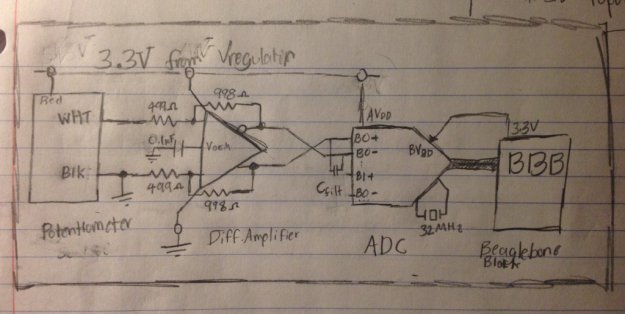
Below is a rough schematic of the major elements in the circuit
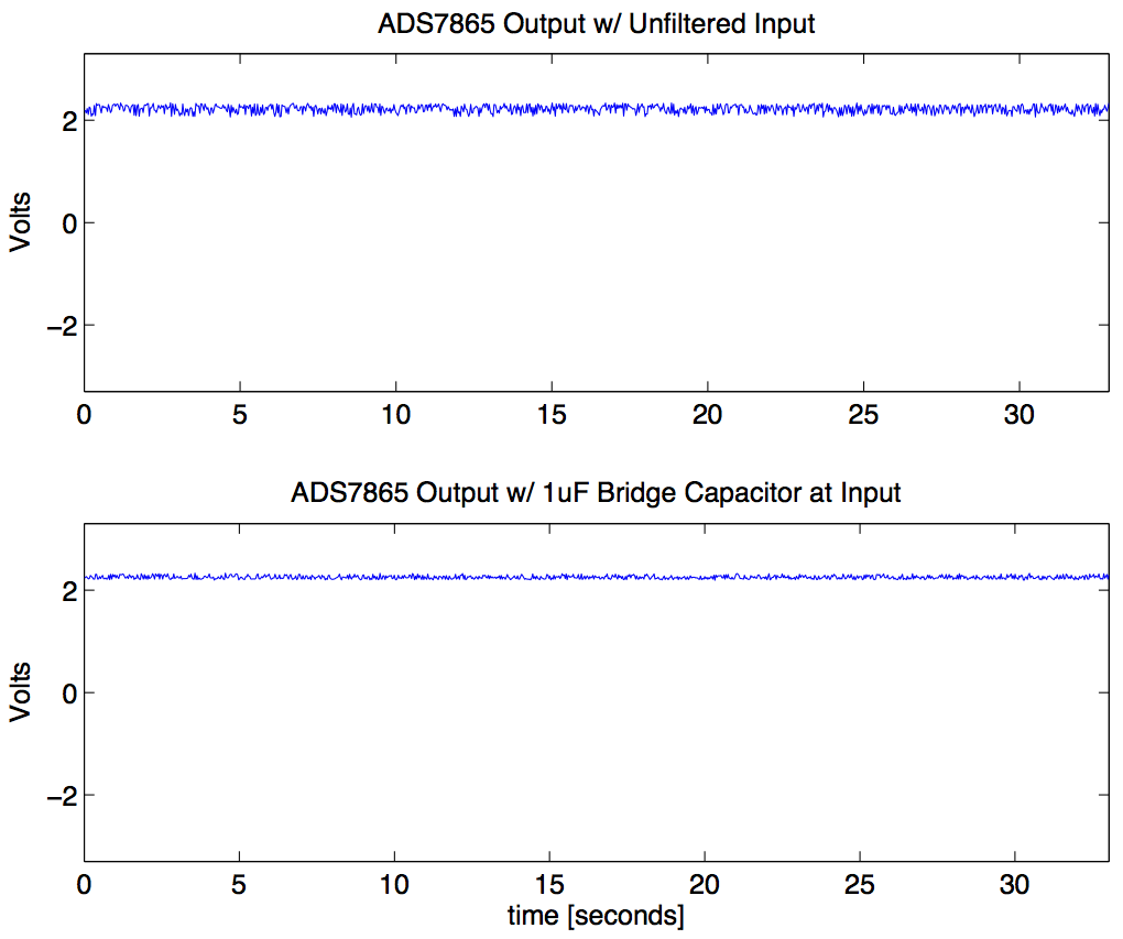
I was able to collect data at a blistering rate of 30 samples per second! Still, this allowed me to examine the noise content of the signal. Below is time-domain plot of the ADC output as its measuring a static potentiometer signal.
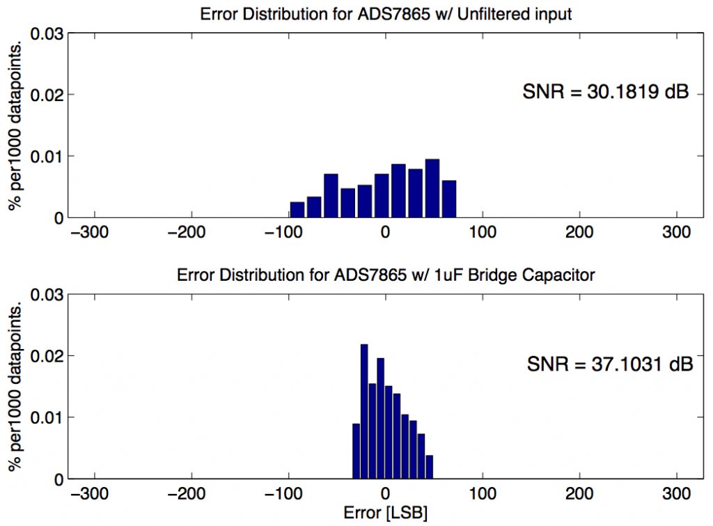
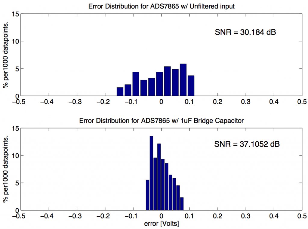
Apparently, noise is visible. The distribution plots help to measure the impact of this noise:
Signal to noise ratio (SNR) is 37dB at best. The ADS7865 spec sheet claims the ADC can attain a maximum SNR of 71dB, so some more work has to be done in order to achieve this level of precision. Namely, the breadboard’s own capacitance and lack of shielding is probably the biggest culprit. It’s undetermined whether the 32MHz clock is coupling EMI into the signal input or not. Possible ways to eliminate noise are hypothesized below:
- PCB Traces. Those long, looping wires on the THS4531 differential outputs are acting like antenna.
- Shield any exposed signal wires.
- Lower some resistor values (for less thermal noise)
Future work will involve establishing a front-end circuit for this ADC, dealing with excess noise, developing a cape for the BBB, and more tests on the BBB.
