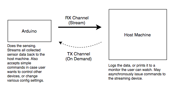
Background
The last post focused on a very early test of the ADS7865, where it was discovered that just controlling the ADC with Sysfs was just too slow to actually work. Since that post, new code has been developed that uses the Beaglebone Black’s (BBB) 200MHz microcontrollers to control the ADC. So far this has resulted in usable throughputs up to 400Ksamps/sec per channel, which is more than sufficient for the application in mind. Discussion of that software will take place near the end of this writeup.
Another important milestone since the last post was that the actual printed circuit board (PCB) design for connecting a pair of hydrophones to the BBB has been completed, fabricated, and populated with all electrical components. The first section of this post will show what it took to build the board.
Constructed PCB
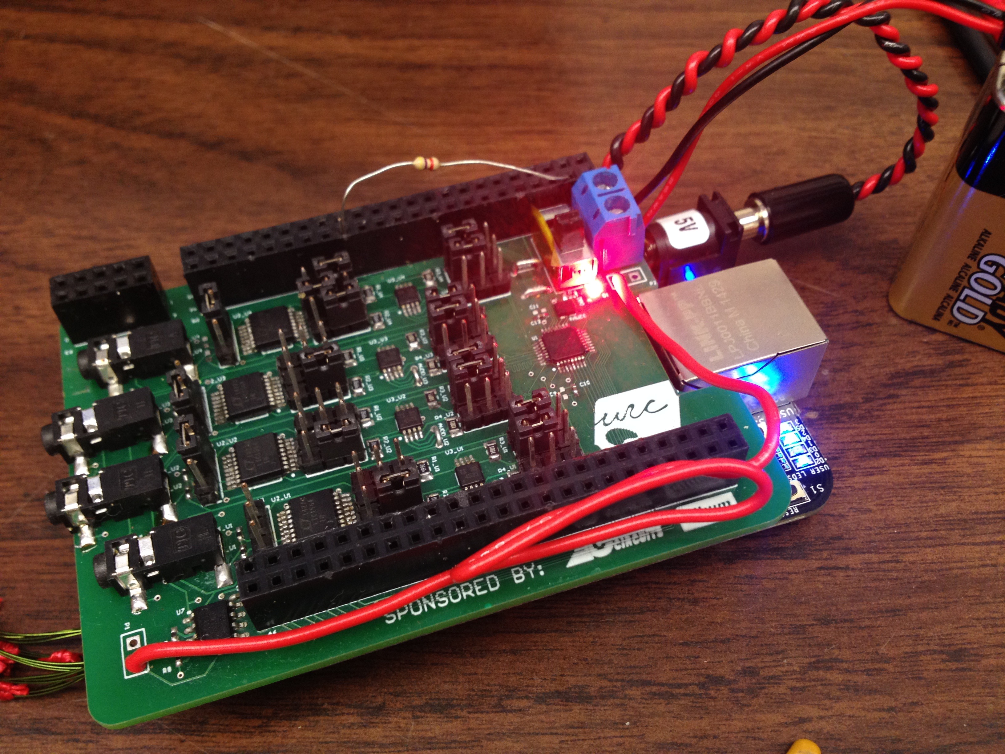
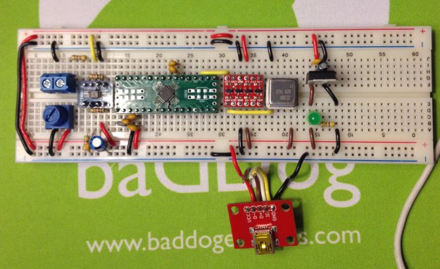
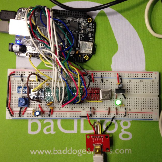
Below is an image of the completed PCB while powered on top of the beaglebone.
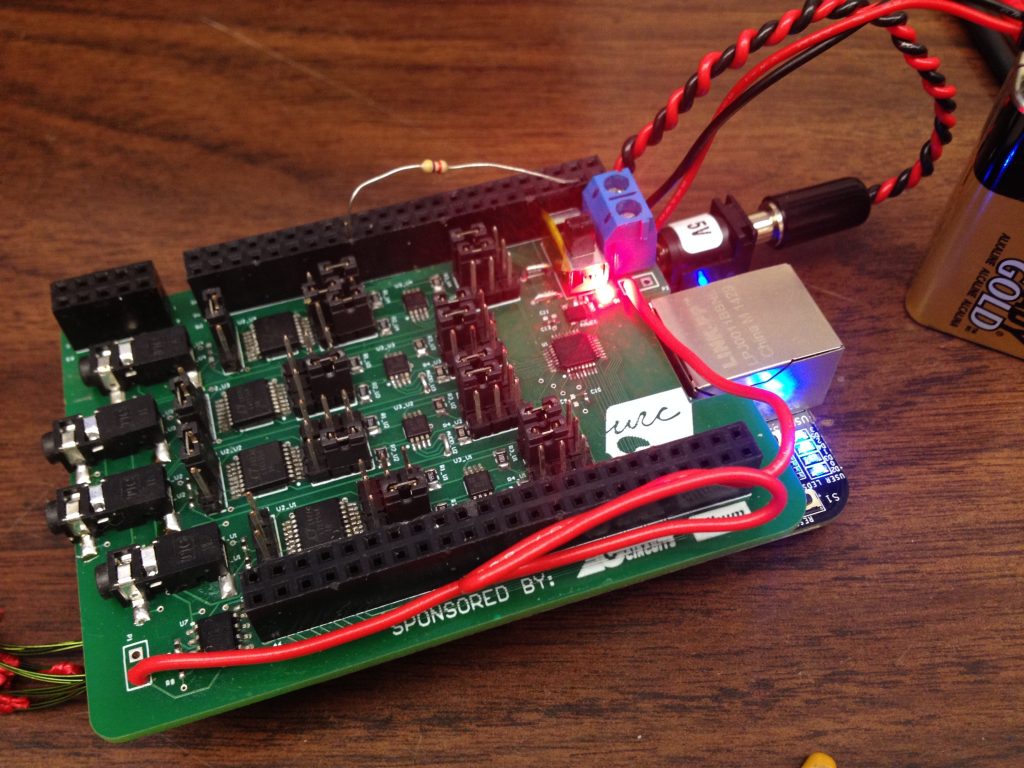
Acoustics board on top of the Beaglebone Black. The 9V battery power supply is just for testing purposes.
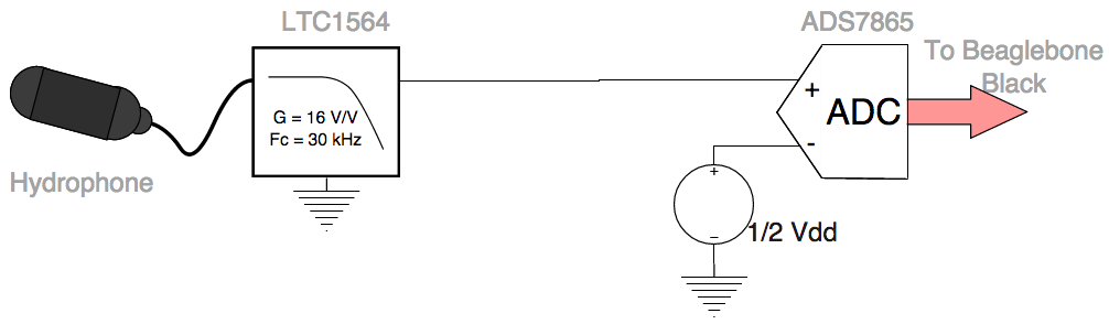
Other than showing the bright power-on indicator LEDs, this image shows off the fact that the original beaglebone header pins are still accessible while this board is attached. If you scan the image from left to right, you’ll trace out the entire analog signal chain of the system: 2.5mm headphone jack inputs –> programmable filter/amplifier chips (LTC1564) –> Differential amplifier ICs (THS4531) –> and a single Analog to Digital Converter IC (ADS7865).
Of course, there were many steps that had to occur before the final board you see above came to be. Check out the slide show below for more detail about the building process.
View post on imgur.com
Code and Application
So, now that the board is all put together, it’s time to discuss the software that interacts with it. Those want to just see the code, all source code for this project can be found at github.com/ncsurobotics/acoustics.
Sampling Code on the PRUs
The main performance challenges of the sampling code were:
- To get it to operate as such a speed that we can sample 4 channels of acoustics data at rate of at least 300KHz per channel (1.2MHz throughput… which is 60% of the maximum capacity of the ADC)
- Transporting the data to application level of the software.
- Establish a simple, easy-to-use means for accessing all the features of ADS7865.
In order to overcome challenges 1 and 2, code was written that made both the BBB’s programmable realtime units (PRUs) work together to interface directly with the ADC. The PRUs are essentially 200MHz microcontrollers. The benefit here is that both PRUs are fast and operate upon assembly code that has a known execution time. Therefore it is possible to write fast code that is guaranteed to complete within “x” amount of time, which is necessary when working with an ADC.
One small difficulty was that the ADS7865 uses a parallel 12 pin parallel data bus to output its samples + 2 other pins to control the ADC itself. This means that it takes 14 pins to control the ADC. However, no PRU on the beaglebone has more than 12 input/output pins. So, we’re forced to write code that gets the PRUs to always work in tandem with each other such that, when combined, they are controlling a total of 14 pins on the ADC.
In the end, the PRU sampling code was able to achieve the following specs
- 1.6MHz maximum throughput rate amongst 4 channels (400KHz per channel).
- The ability to store a maximum of 15,000 samples to a region of memory accessible to the user on the application layer of the software.
- The ability to invoke a sampling trigger that works much like the trigger on an oscilloscope.
All the PRU code can be found in the github repository
Application Layer Code
Another set of code that had to be written was the application layer code, which allows us to:
- Modify the ADS7865’s sequencer, which determines how many and what order the ADS7865 will sample it’s 4 channels.
- Modify the sampling rate for the ADS7865.
- Pull data that the PRUs collect from the ADS7865 from memory
- Process such data.
- Control the programmable amplifiers/filters
Essentially, these bullets attend to all the aspect of challenge #3 described about. All of this code was written in python so far, and it can be found on the github repository.
Signal Capture
Method
It’s desirable to attain some objective measurement of how much noise is present in the system, and well well each component suppresses that noise. To fulfill this desire, the following was done:
- Attach a hydrophone to the input end of the circuit.
- Configure circuit such that a particular signal path is selected out of the several that are possible.
- Rest the hydrophone is a place where it won’t be accidentally disturbed and is as far away as possible from any noise sources.
- Record 12,500 samples of data at 800KHz of the hydrophone just sitting undisturbed. Inspect a plot of the data over time.
- Compute key measures of merit: RMS value of the noise signal, signal to noise ratio (RMS)
- Assume error is any deviation from the mean value of the static signal, by which a distribution plot can be created to show the overall picture behind this error. Inspect this plot.
- Repeat steps 3 – 6 for all the other possible configurations of the signal chain.
Concerning step 5, the standard equation for calculating the RMS value of an arbitrary signal is
[latex]V_{RMS} = \left ( \frac{1}{T}\int_{0}^{T}V_{sig}^{2}(t)dt\right )^\frac{1}{2}[/latex]
where T is the period of time by which the data was collected and [latex]V_{sig}(t)[/latex] represents the signal. Computationally, we can perform this measurement by rewriting the equation as.
[latex]V_{RMS} =\sqrt{\frac{1}{\textup{T}}\sum_{m=0}^{M}( V_{sig}^{2}[m]\textup{Ts} )}[/latex]
whereas M is the number of samples collected and Ts is the sampling period. [latex]V_{sig}[m][/latex] represents the voltage value for sample m.
And lastly for part 5 is signal to noise ration (SNR). The equation for this is
[latex]\textup{SNR} = 20\log_{10}\left ( \frac{\textup{RMS Value of input}}{\textup{RMS Value of noise}} \right )[/latex]
For our purposes, we’ll be computing maximum possible SNR. The full scale voltage range of the system is ±2.5V, so we’ll just assume “RMS Value of input” to be the RMS value of a 2.5V sinusoid, which is just [latex]2.5 / \sqrt{2} \ \textup{Vrms}[/latex], or about 1.77 Vrms.
Results
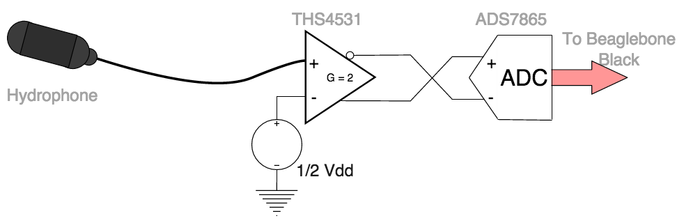
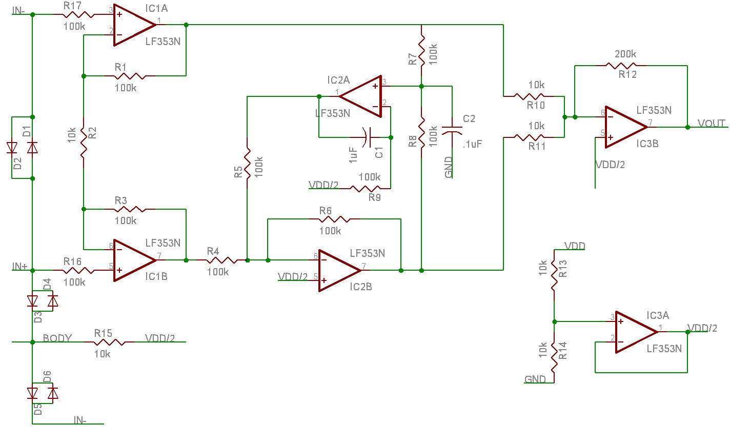
Below is a block diagram of the full signal chain of the acoustics system, along with the data acquired to determine how much noise is present when the system is in this configuration.
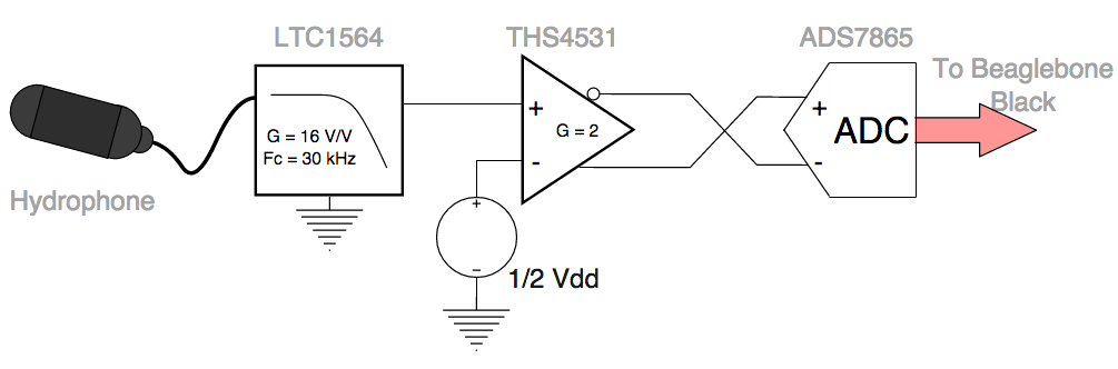
Full signal chain of the acoustics system.
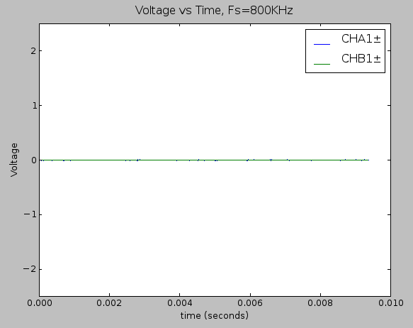
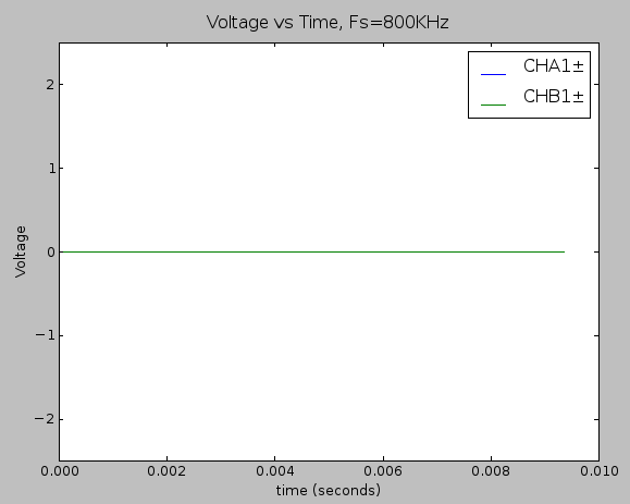
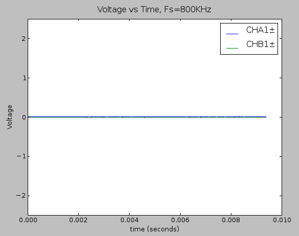
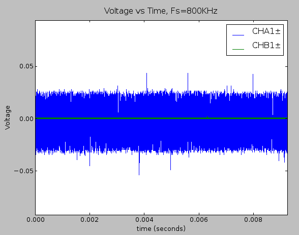
Time domain plot of the static noise measurement within the full signal range of ±2.5V (full signal chain).
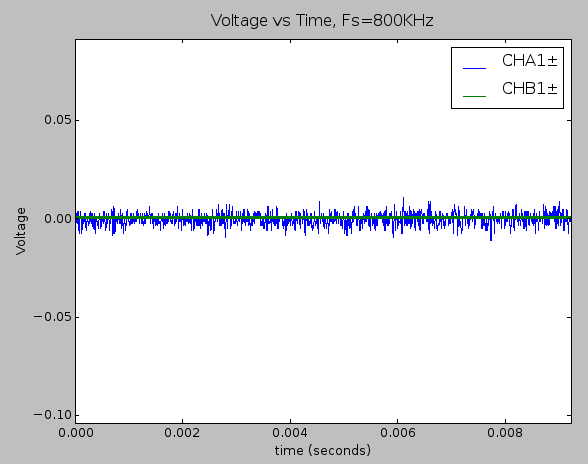
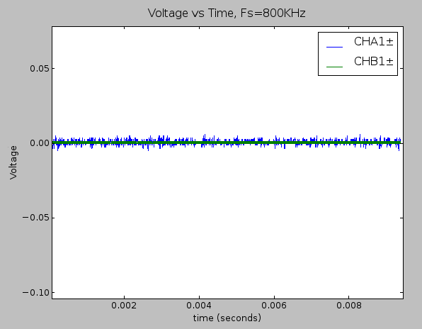
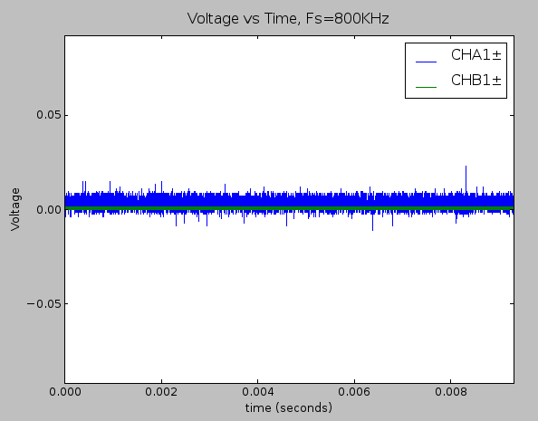
Zoomed in version of the plot shown above.
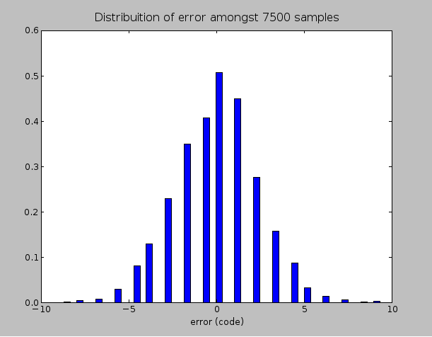
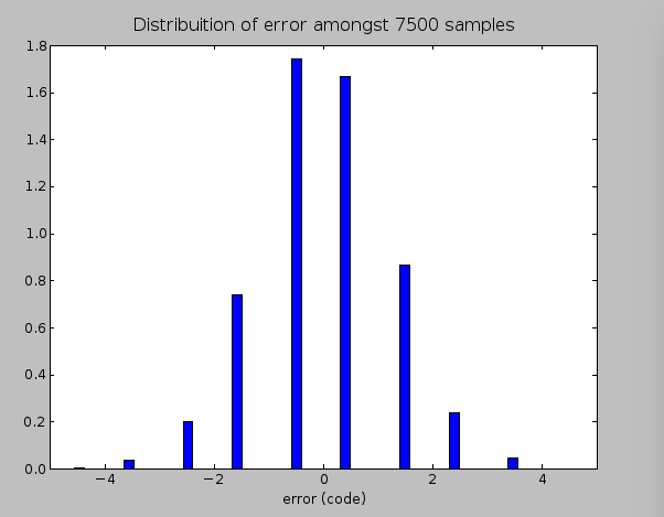
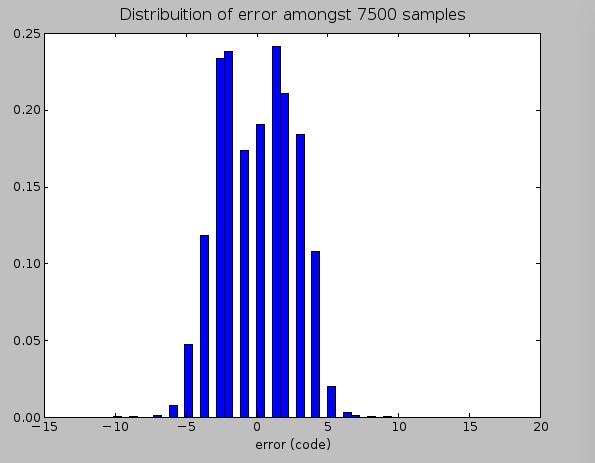
Distribution of error when the full signal chain is involved. Noise content was about 2.9mVRMS (2.4 binary code values). This corresponds to a maximum signal to noise ratio of 58dB.
Now, let’s remove the differential amplifier from the signal chain (see block diagram below) and redo our static noise measurement to see what kind of effect this component had.
Block diagram representing the removal of the differential amplifier from the signal chain.
Time domain plot of the static noise measurement within the full ±2.5V signal range while using only the filter in the signal chain.
Zoomed in version of the plot shown above.
Distribution of error when the only the filter is involved, as shown in the schematic above. Noise content was about 1.5mVRMS (about 1.2 binary code values). This corresponds to a maximum signal to noise ratio of 61dB.
The data shows that just removing the THS4531 reduced the RMS noise content by a factor of 2. This make sense because this part of the circuit is set up with a gain of 2, which means that within the bandwidth spanning DC to ~30KHz, the THS4531 isn’t really adding any additional noise to the system that wasn’t already there to begin with.
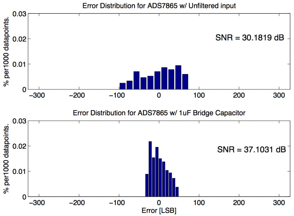
Now we’ll put the THS4531 back in the signal chain and remove the LTC1564 programmable filter instead, as shown below.
Block diagram representing the removal of just the LTC1564 from the signal chain.
And here is data from performing the same static noise measurement on the circuit.
Time domain plot of the static noise measurement within the full ±2.5V (using only the THS4531 in the signal chain).
Zoomed in version of the plot shown above.
Distribution of error when the only the THS4531 is involved in the signal chain, as shown in the schematic above. Noise content was about 3.2mVRMS (about 2.6 binary code values). This corresponds to a signal to noise ratio of 55dB.
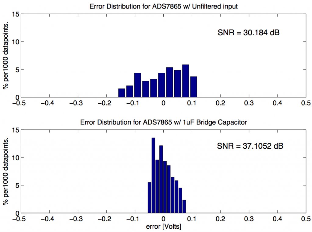
And finally, we remove the differential amplifier from the signal chain so that the ADC picks up the raw hydrophone noise signal.
Block diagram representing the removal of all components from the signal chain. The ADS7865 receives a raw, single-ended hydrophone signal.
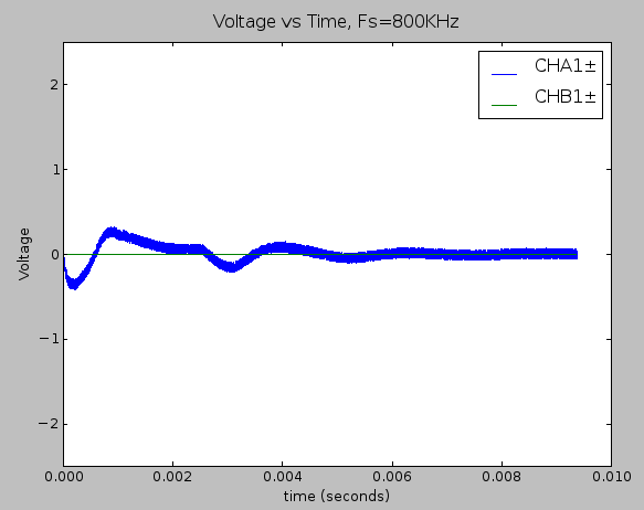
Time domain plot of the static noise measurement within the full ±2.5V while passing the raw hydrophone signal on the signal chain.
Zoomed in version of the plot shown above.
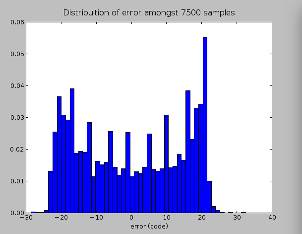
Distribution of error when the only the THS4531 is involved in the signal chain, as shown in the schematic above. Noise content was about 18mVRMS (about 15 binary code values). This corresponds to an SNR of 40dB
One takeaway here is that passing an unconditioned, single-ended hydrophone signal to the ADC results in a lot of noise, and that’s with no amplification whatsoever. With the proper components, we were able to amplify the hydrophone signal while reducing a huge amount on noise in the system. For reference here’s what tapping on the hydrophone looks like unconditioned
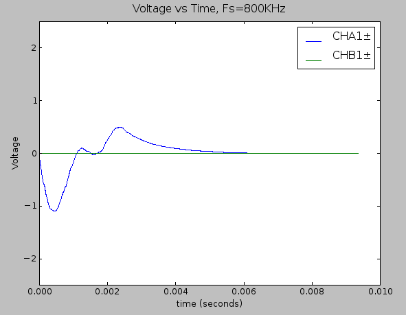
System response to a single tap on the hydrophone with no signal conditioning electronics are involved.
And for comparison, here is the system response to a similar tap when both the LTC1564 and THS4531 are involved in conditioning the single.
System response to a single tap on the hydrophone with both the LTC1564 and THS4531 are involved.
Just to give one more example of what the system’s output looks like, here’s a recent lab test where a clean 5KHz sinusoidal signal is injected into 2 of the 4 available inputs (no hydrophone was used in this case, but both the LTC1564 and THS4531 were involve with conditioning the signal).
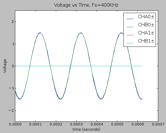
Data as recorded by the ADC after injecting a 5KHz signal into system inputs CHA0 and CHB0
Closing Remarks
More development and testing is underway. The next post will center around testing this system with real hydrophones, and some discussion of how the we use this system to determine the location of an ultrasonic pinger in the water.
Appendix A: Missing Vref Capacitor
The datasheet for the ADS7865 has a pretty clear recommendation about pin 1 of the ADC, the reference input (REF_in):
The reference input is not buffered and is directly connected to the ADC. The converter generates spikes on the reference input voltage because of internal switching. Therefore, an external capacitor to the analog ground (AGND) should be used to stabilize the reference input voltage. This capacitor should be at least 470nF… —ADS7865 Datasheet
It turns out that while building up this board, I initially forgot to add this very capacitor. For the sake of science, I document what your signal will look like if you make the same mistake I did.
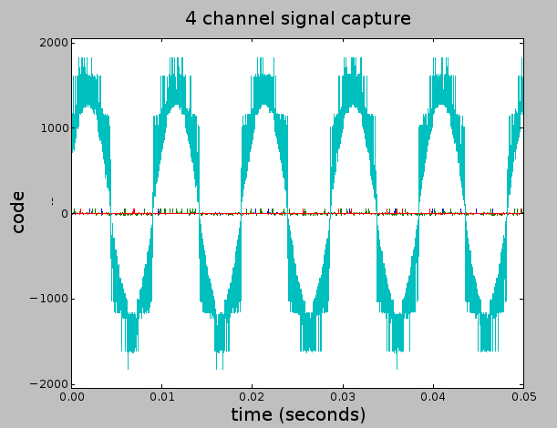
Failing to add a capacitor buffer on ADCs Vref buffer will cause a very characteristic noise pattern.
From this picture, one can see exactly what the datasheet is talking about especially with the red, green, and blue traces around 0V. On another note, the teal trace brings up something interesting. We’ve essentially magnified the amount of error that comes from error in the reference input. Its interesting to note that the zero-crossing of the teal signal has almost no noise content. However, the further the 0V, the more noise it accumulates. This is due to the fact that output code comes from the following equation universal to nearly all n-bit ADCs:
[latex]Output = \frac{2^n}{V_{ref}}V_{in.ADC}\ [\textup{bits}][/latex]
Whereas Vref is the reference input voltage, Vin.ADC is the voltage present at the ADC inputs, and Output is the digital value that is read out to the beaglebone. We see no noise in the signal at 0V because Vin.ADC = 0 at that point, and thus any variation in Vref does not effect the output. As soon as Vin.ADC is non-zero, variation in Vref will start to effect the output. The further Vin.ADC is from zero, the more apparent this effect become.
For those who are more interested in the exact nature of how error in Vref effects the output, consider the equation below
[latex]E_{code} = -\frac{2^nV_{in}}{V_{ref}^2}E_{ref}\ [\textup{bits}][/latex]
Whereas E_code is the error in the output code and E_ref is the error in Vref. This equation came just from taking the derivative of the previous equation with respect to Vref. Maybe this information may come in handy when it comes to minimizing error in another ADC system, and it looks like the biggest source of error might be in the Vref signal.


