Category Archives: Projects

FloorBot

Some of us may say at one point of our lives: “Gee, I wish I had a robot that could fit in my small apartment and that would be so fun to drive around right now. Plus, if I  feel up to it, I could challenge myself to see if I can get it to roam around autonomously!”

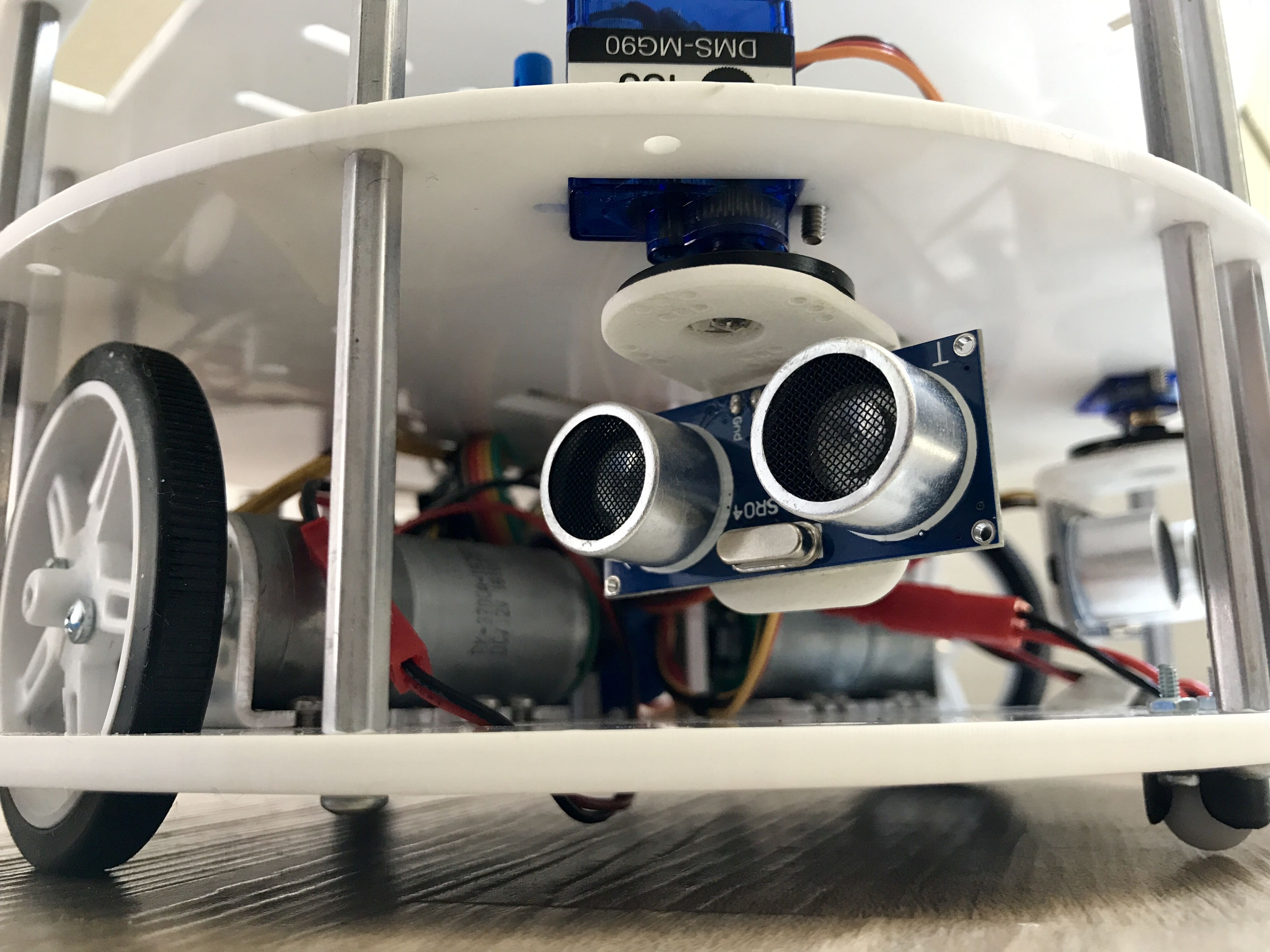
This project may be the fruition of that idea. Meet FloorBot: a two wheeled robot that can drive through any hallway of your carefully sized living space. Measuring 12″ in diameter with a zero degree turning radius, it could navigate around any corner or coffee table with ease. Equipped with two servo actuated ultrasonic distance sensors, it can detect and avoid obstacles that enter in its path under its own (partial) autonomous control.   I learned a little bit about the ESP32 over the course of this project, so FloorBot also has WiFi connectivity and browser based control for easy  use and loss of productivity while attempting new driving patterns.

FloorBot, in its present form, is a fun prototype that was built using off the shelf electronics in order to get running as quickly as possible. It is by no means perfect. There is an ongoing effort to achieve fully autonomous roaming for this vehicle, which is also proving to be quite challenging under limited hardware selected for this prototype. This page is merely a rolling log of FloorBot’s achievements, highlights, and construction. As more development is done over the course of FloorBot’s lifetime, this page will be updated accordingly.

Floorbot’s Achievements

Autonomous Wall Avoidance

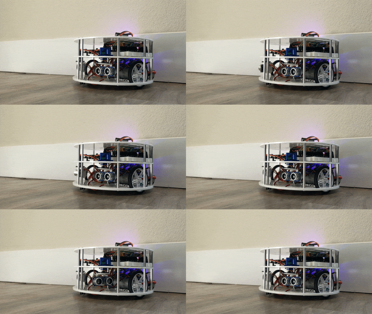
Wall avoidance is achieved by the onboard ultrasonic distance sensors. As shown in the video below, the distance sensors may be set at fixed angles, or they may be pivoted in order to cover the front and sides of the robot.

WiFi Control

Control over WiFi was achieved using an ESP32 dev board and some modified javascript from jeromeetienne’s virtualjoystick.js library. It really makes a huge difference in testing out vehicle controls and movements. Even though there’s a lot of latency over the WiFi network (as observed in the video below) as least there’s a way to easily position the vehicle in new locations without even leaving the computer screen.

Build Details

Powertrain and Power Electronics

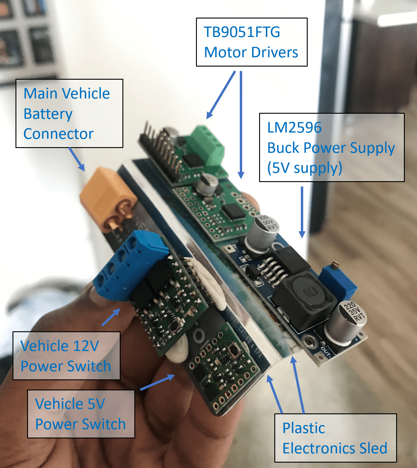
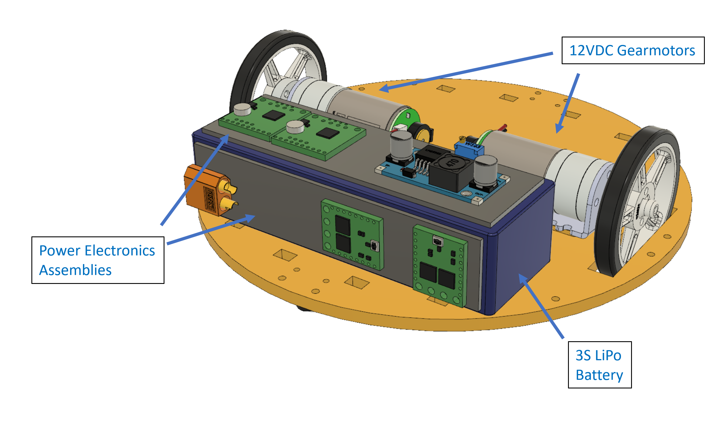
The robot powertrain is located on the bottom shelf of the vehicle. It consist of two DC gearmotor with magnetic rotary encoders, a power electronics assembly, and a 3S lipo battery.

One cool thing about the power electronics assembly is that it slides directly on top of the LiPo Battery. This was done in an effort to minimize the length of power cabling and to keep high voltage electronics as far away from the low voltage digital control electronics as possible.

The picture below captures the power electronics assembly in an early prototyping phase, prior to soldering on any wires. If you look closely enough, you can see how I made the electronics sled: by cutting up an old gift card and linking the two half together with clear packing tape.

This ended up making for a cool flexible PCB assembly that slides right on top of the battery pack. The flexible nature of this assembly also helped during the wiring process, as I was able to lay it flat on a table for solder prior to inserting it in the vehicle.

Servo mounted distance sensors

Distance sensors were mounted on servos in order to give FloorBot ability point them in direction of travel. This was meant to save on costs of having to build some large circular array of +3 SONARs, or having to invest in some LIDAR based solution.

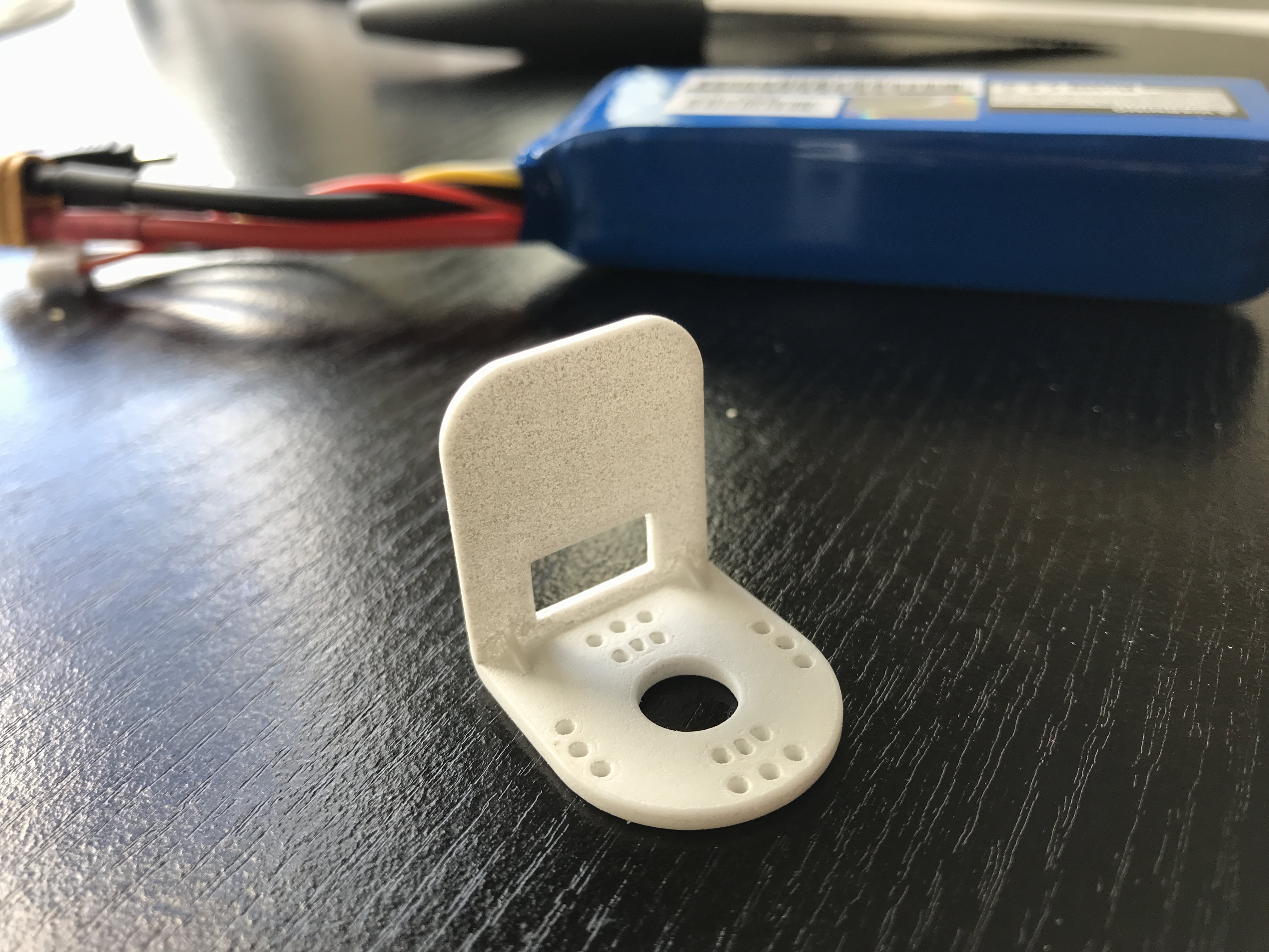
In order to mount the distance sensors to the servos, small L-brackets were 3D printed for each servo. The bracket contains holes for afixing the bracket to your standard servo horn, and a larger rectangular cutout for feeding wiring into the distance sensor connection pins.

Beaglebone Black Underwater Acoustics System: Part 2

Background

The last post focused on a very early test of the ADS7865, where it was discovered that just controlling the ADC with Sysfs was just too slow to actually work. Since that post, new code has been developed that uses the Beaglebone Black’s (BBB) 200MHz microcontrollers to control the ADC. So far this has resulted in usable throughputs up to 400Ksamps/sec per channel, which is more than sufficient for the application in mind. Discussion of that software will take place near the end of this writeup.

Another important milestone since the last post was that the actual printed circuit board (PCB) design for connecting a pair of hydrophones to the BBB has been completed, fabricated, and populated with all electrical components. The first section of this post will show what it took to build the board.

Constructed PCB

Below is an image of the completed PCB while powered on top of the beaglebone.
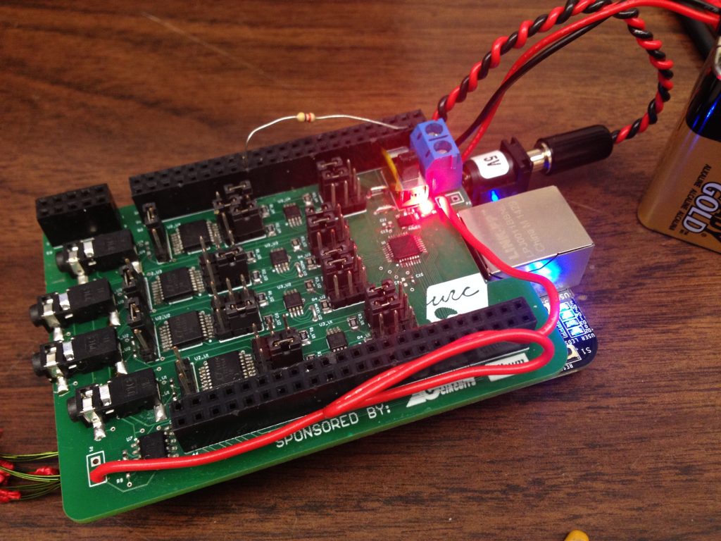
Acoustics board on top of the Beaglebone Black.

Acoustics board on top of the Beaglebone Black. The 9V battery power supply is just for testing purposes.

Other than showing the bright power-on indicator LEDs, this image shows off the fact that the original beaglebone header pins are still accessible while this board is attached. If you scan the image from left to right, you’ll trace out the entire analog signal chain of the system: 2.5mm headphone jack inputs –> programmable filter/amplifier chips (LTC1564) –> Differential amplifier ICs (THS4531) –> and a single Analog to Digital Converter IC (ADS7865).

Of course, there were many steps that had to occur before the final board you see above came to be. Check out the slide show below for more detail about the building process.

View post on imgur.com

Code and Application

So, now that the board is all put together, it’s time to discuss the software that interacts with it. Those want to just see the code, all source code for this project can be found at github.com/ncsurobotics/acoustics.

Sampling Code on the PRUs

The main performance challenges of the sampling code were:

  1. To get it to operate as such a speed that we can sample 4 channels of acoustics data at rate of at least 300KHz per channel (1.2MHz throughput… which is 60% of the maximum capacity of the ADC)
  2. Transporting the data to application level of the software.
  3. Establish a simple, easy-to-use means for accessing all the features of ADS7865.

In order to overcome challenges 1 and 2, code was written that made both the BBB’s programmable realtime units (PRUs) work together to interface directly with the ADC. The PRUs are essentially 200MHz microcontrollers. The benefit here is that both PRUs are fast and operate upon assembly code that has a known execution time. Therefore it is possible to write fast code that is guaranteed to complete within “x” amount of time, which is necessary when working with an ADC.

One small difficulty was that the ADS7865 uses a parallel 12 pin parallel data bus to output its samples + 2 other pins to control the ADC itself. This means that it takes 14 pins to control the ADC. However, no PRU on the beaglebone has more than 12 input/output pins. So, we’re forced to write code that gets the PRUs to always work in tandem with each other such that, when combined, they are controlling a total of 14 pins on the ADC.

In the end, the PRU sampling code was able to achieve the following specs

  • 1.6MHz maximum throughput rate amongst 4 channels (400KHz per channel).
  • The ability to store a maximum of 15,000 samples to a region of memory accessible to the user on the application layer of the software.
  • The ability to invoke a sampling trigger that works much like the trigger on an oscilloscope.

All the PRU code can be found in the github repository

Application Layer Code

Another set of code that had to be written was the application layer code, which allows us to:

  • Modify the ADS7865’s sequencer, which determines how many and what order the ADS7865 will sample it’s 4 channels.
  • Modify the sampling rate for the ADS7865.
  • Pull data that the PRUs collect from the ADS7865 from memory
  • Process such data.
  • Control the programmable amplifiers/filters

Essentially, these  bullets attend to all the aspect of challenge #3 described about. All of this code was written in python so far, and it can be found on the github repository.

Signal Capture

Method

It’s desirable to attain some objective measurement of how much noise is present in the system, and well well each component suppresses that noise. To fulfill this desire, the following was done:

  1. Attach a hydrophone to the input end of the circuit.
  2. Configure circuit such that a particular signal path is selected out of the several that are possible.
  3. Rest the hydrophone is a place where it won’t be accidentally disturbed and is as far away as possible from any noise sources.
  4. Record 12,500 samples of data at 800KHz of the hydrophone just sitting undisturbed. Inspect a plot of the data over time.
  5. Compute key measures of merit: RMS value of the noise signal, signal to noise ratio (RMS)
  6. Assume error is any deviation from the mean value of the static signal, by which a distribution plot can be created to show the overall picture behind this error. Inspect this plot.
  7. Repeat steps 3 – 6 for all the other possible configurations of the signal chain.

Concerning step 5, the standard equation for calculating the RMS value of an arbitrary signal is

[latex]V_{RMS} = \left ( \frac{1}{T}\int_{0}^{T}V_{sig}^{2}(t)dt\right )^\frac{1}{2}[/latex]

where T is the period of time by which the data was collected and [latex]V_{sig}(t)[/latex] represents the signal. Computationally, we can perform this measurement by rewriting the equation as.

[latex]V_{RMS} =\sqrt{\frac{1}{\textup{T}}\sum_{m=0}^{M}( V_{sig}^{2}[m]\textup{Ts} )}[/latex]

whereas M is the number of samples collected and Ts is the sampling period. [latex]V_{sig}[m][/latex] represents the voltage value for sample m.

And lastly for part 5 is signal to noise ration (SNR). The equation for this is

[latex]\textup{SNR} = 20\log_{10}\left ( \frac{\textup{RMS Value of input}}{\textup{RMS Value of noise}} \right )[/latex]

For our purposes, we’ll be computing maximum possible SNR. The full scale voltage range of the system is ±2.5V, so we’ll just assume “RMS Value of input” to be the RMS value of a 2.5V sinusoid, which is just [latex]2.5 / \sqrt{2} \ \textup{Vrms}[/latex], or about 1.77 Vrms.

Results

Below is a block diagram of the full signal chain of the acoustics system, along with the data acquired to determine how much noise is present when the system is in this configuration.

Full signal chain of the acoustics system.
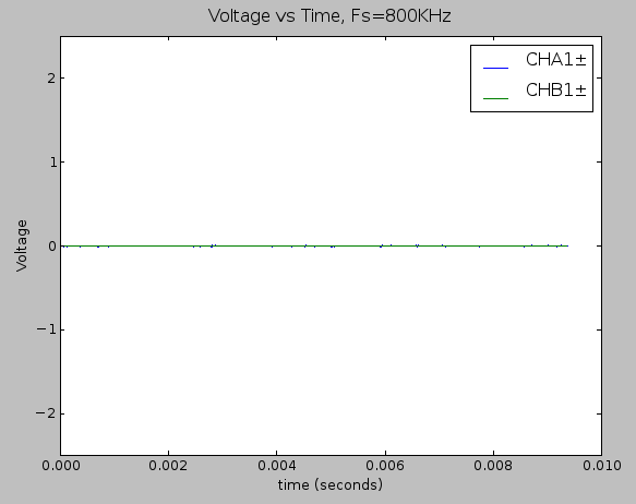
Full signal chain of the acoustics system.

Time domain plot of the static noise measurement (full signal chain)

Time domain plot of the static noise measurement within the full signal range of ±2.5V (full signal chain).
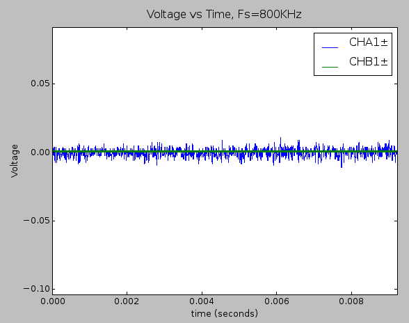
Zoomed in version of the plot shown above.
Zoomed in version of the plot shown above.

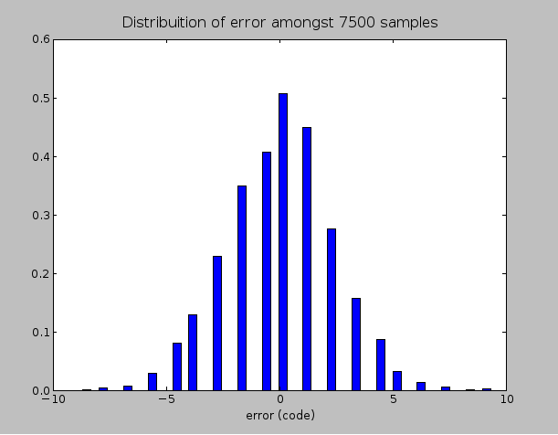
Distribution of error when the full signal chain is involved. Noise content was about 2.9mVRMS (2.4 bits)

Distribution of error when the full signal chain is involved. Noise content was about 2.9mVRMS (2.4 binary code values). This corresponds to a maximum signal to noise ratio of 58dB.

Now, let’s remove the differential amplifier from the signal chain (see block diagram below) and redo our static noise measurement to see what kind of effect this component had.

Block diagram representing the removal of the differential amplifier from the signal chain.
Block diagram representing the removal of the differential amplifier from the signal chain.

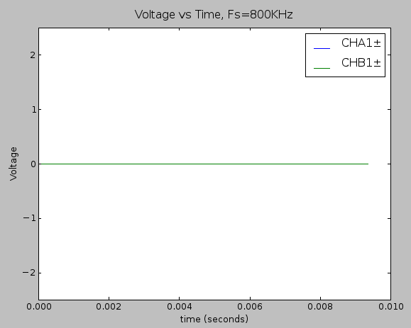
Time domain plot of the static noise measurement (using only the filter in the signal chain).

Time domain plot of the static noise measurement within the full ±2.5V signal range while using only the filter in the signal chain.
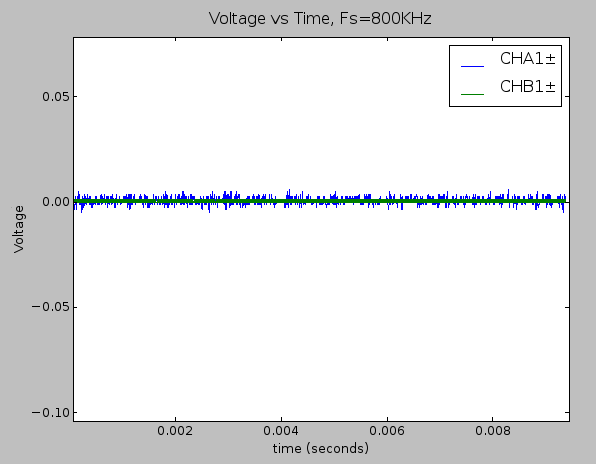
Zoomed in version of the plot shown above.
Zoomed in version of the plot shown above.

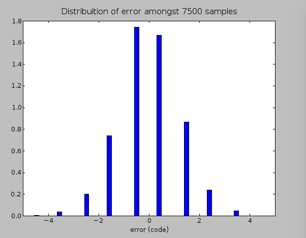
Distribution of error when the only the filter is involved, as shown in the schematic above. Noise content was about 1.5mVRMS (1.2 bits)

Distribution of error when the only the filter is involved, as shown in the schematic above. Noise content was about 1.5mVRMS (about 1.2 binary code values). This corresponds to a maximum signal to noise ratio of 61dB.

The data shows that just removing the THS4531 reduced the RMS noise content by a factor of 2. This make sense because this part of the circuit is set up with a gain of 2, which means that within the bandwidth spanning DC to ~30KHz, the THS4531 isn’t really adding any additional noise to the system that wasn’t already there to begin with.

Now we’ll put the THS4531 back in the signal chain and remove the LTC1564 programmable filter instead, as shown below.

Block diagram representing the removal of just the LTC1564 from the signal chain.

Block diagram representing the removal of just the LTC1564 from the signal chain.

And here is data from performing the same static noise measurement on the circuit.
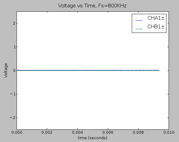
Time domain plot of the static noise measurement (using only the THS4531 in the signal chain).

Time domain plot of the static noise measurement within the full ±2.5V (using only the THS4531 in the signal chain).
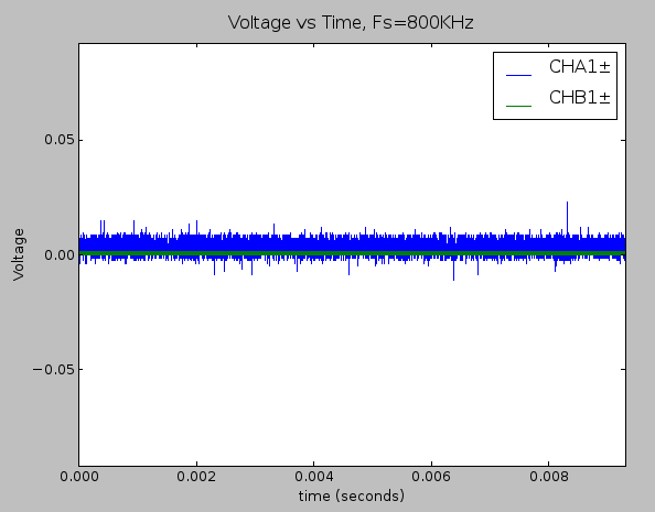
Zoomed in version of the plot shown above.
Zoomed in version of the plot shown above.

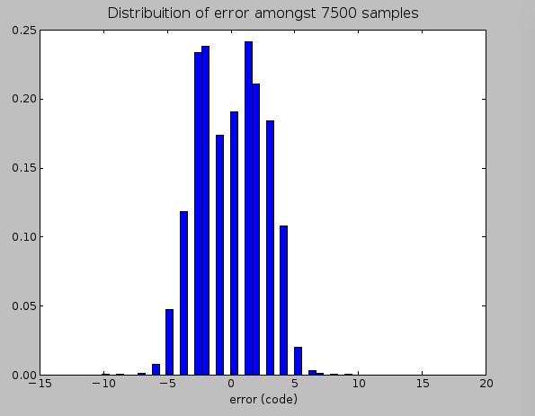
Distribution of error when the only the THS4531 is involved in the signal chain, as shown in the schematic above. Noise content was about 3.2mVRMS (about 2.6 bits)

Distribution of error when the only the THS4531 is involved in the signal chain, as shown in the schematic above. Noise content was about 3.2mVRMS (about 2.6 binary code values). This corresponds to a signal to noise ratio of 55dB.

And finally, we remove the differential amplifier from the signal chain so that the ADC picks up the raw hydrophone noise signal.
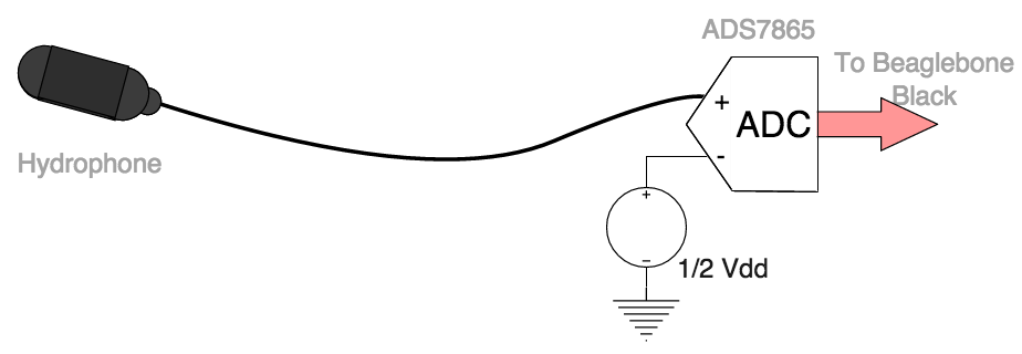
Block diagram representing the removal of all components from the signal chain. The ADS7865 receives a raw, single-ended hydrophone signal.
Block diagram representing the removal of all components from the signal chain. The ADS7865 receives a raw, single-ended hydrophone signal.

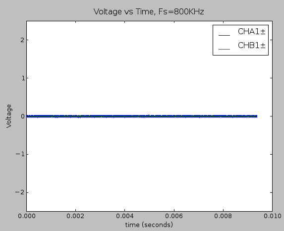
Time domain plot of the static noise measurement within the full ±2.5V while passing the raw hydrophone signal on the signal chain.
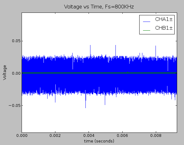
Time domain plot of the static noise measurement within the full ±2.5V while passing the raw hydrophone signal on the signal chain.

Zoomed in version of the plot shown above.
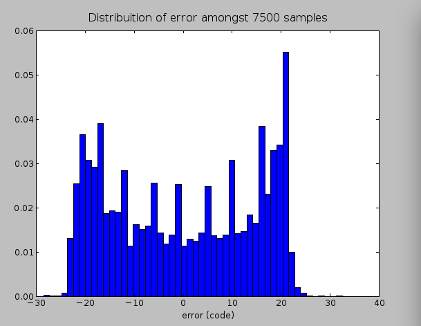
Zoomed in version of the plot shown above.

Distribution of error when the only the THS4531 is involved in the signal chain, as shown in the schematic above. Noise content was about 18mVRMS (about 15 bits)

Distribution of error when the only the THS4531 is involved in the signal chain, as shown in the schematic above. Noise content was about 18mVRMS (about 15 binary code values). This corresponds to an SNR of 40dB

One takeaway here is that  passing an unconditioned, single-ended hydrophone signal to the ADC results in a lot of noise, and that’s with no amplification whatsoever. With the proper components, we were able to amplify the hydrophone signal while reducing a huge amount on noise in the system. For reference here’s what tapping on the hydrophone looks like unconditioned
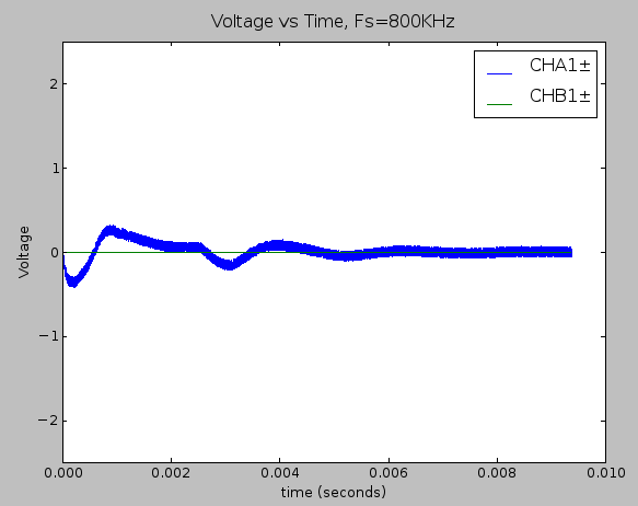
System response to a single tap on the hydrophone with no signal conditioning electronics are involved.

System response to a single tap on the hydrophone with no signal conditioning electronics are involved.

And for comparison, here is the system response to a similar tap when both the LTC1564 and THS4531 are involved in conditioning the single.
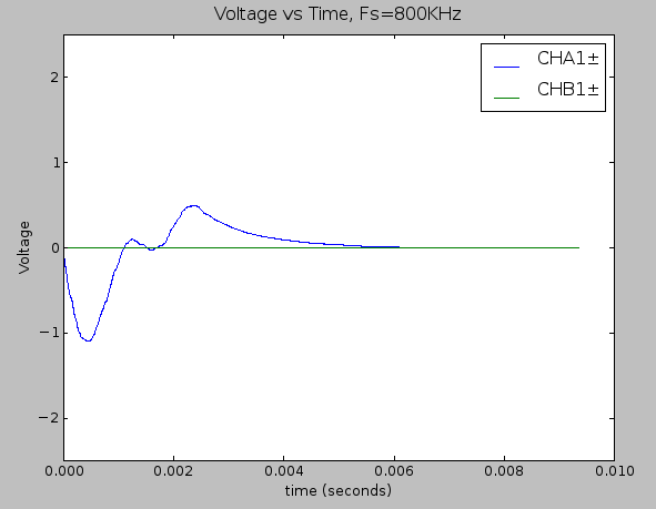
System response to a single tap on the hydrophone with both the LTC1564 and THS4531 are involved.

System response to a single tap on the hydrophone with both the LTC1564 and THS4531 are involved.

Just to give one more example of what the system’s output looks like, here’s a recent lab test where a clean 5KHz sinusoidal signal is injected into 2 of the 4 available inputs (no hydrophone was used in this case, but both the LTC1564 and THS4531 were involve with conditioning the signal).
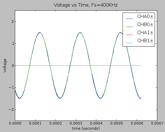
Data as recorded by the ADC after injecting a 5KHz signal into system inputs CHA0 and CHB0.

Data as recorded by the ADC after injecting a 5KHz signal into system inputs CHA0 and CHB0

Closing Remarks

More development and testing is underway. The next post will center around testing this system with real hydrophones, and some discussion of how the we use this system to determine the location of an ultrasonic pinger in the water.

Appendix A: Missing Vref Capacitor

The datasheet for the ADS7865 has a pretty clear recommendation about pin 1 of the ADC, the reference input (REF_in):

The reference input is not buffered and is directly connected to the ADC. The converter generates spikes on the reference input voltage because of internal switching. Therefore, an external capacitor to the analog ground (AGND) should be used to stabilize the reference input voltage. This capacitor should be at least 470nF… —ADS7865 Datasheet

It turns out that while building up this board, I initially forgot to add this very capacitor.  For the sake of science, I document what your signal will look like if you make the same mistake I did.
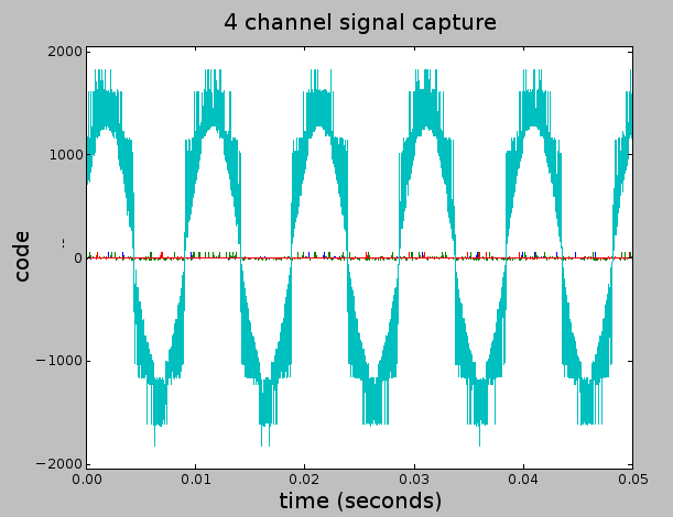
Failing to add a capacitor buffer on ADCs Vref buffer will cause a very characteristic noise pattern.

From this picture, one can see exactly what the datasheet is talking about especially with the red, green, and blue traces around 0V. On another note, the teal trace brings up something interesting. We’ve essentially magnified the amount of error that comes from error in the reference input. Its interesting to note that the zero-crossing of the teal signal has almost no noise content. However, the further the 0V, the more noise it accumulates. This is due to the fact that output code comes from the following equation universal to nearly all n-bit ADCs:

[latex]Output = \frac{2^n}{V_{ref}}V_{in.ADC}\ [\textup{bits}][/latex]

Whereas Vref is the reference input voltage, Vin.ADC is the voltage present at the ADC inputs, and Output is the digital value that is read out to the beaglebone. We see no noise in the signal at 0V because Vin.ADC = 0 at that point, and thus any variation in Vref does not effect the output. As soon as Vin.ADC is non-zero, variation in Vref will start to effect the output. The further Vin.ADC is from zero, the more apparent this effect become.

For those who are more interested in the exact nature of how error in Vref effects the output, consider the equation below

[latex]E_{code} = -\frac{2^nV_{in}}{V_{ref}^2}E_{ref}\ [\textup{bits}][/latex]

Whereas E_code is the error in the output code and E_ref is the error in Vref. This equation came just from taking the derivative of the previous equation with respect to Vref. Maybe this information may come in handy when it comes to minimizing error in another ADC system, and it looks like the biggest source of error might be in the Vref signal.
Portable EKG

Completed circuit

Conception:

This project began from an oversimplification. One day, I wondered: “How hard can it be to make an EKG? How hard is it to amplify the heart’s electrical signal? It can’t be too expensive to make one myself, right?” A quick search on the internet gave me the motivation to build one myself, and so I did. This page is meant to document the stages that I went through in building this EKG for a couple dollars. Anyone can do this, and as such, I encourage anyone to take up a similar project as a fun way to practice their programming and circuit building skills.

Hold up, It’s safety time. While I do support any opportunity to learn circuits and experiment, there’s something about safety that has to be said about this particular project.  This EKG circuit has no electrical isolation from whatever it is connected to.

Because of this, everyone needs to know that this EKG should never be used on a desktop computer, or a laptop charging off a wall wart of any kind. This is because if the computer’s power supply is poorly designed, or even if some random accident occurs, there’s the potential for mains electricity to travel from the power supply to the computer, through the audio port, through the EKG, to your body. This is what is known as electrocution, and it is potentially fatal. 120VAC is not something you want across your chest.

As such, I only really recommend building this circuit if A) You’re willing to come up with some form of isolation to protect yourself, or B) You understand all the risks involved, and you’ll do everything in your ability to avoid using alongside any mains power device. In my case, I only use this circuit along side a laptop computer that is working off of battery power only. I’d put my charging cable somewhere far away when messing around with this circuit.

1) Drafting a few goals:

In the couple of days that followed the conception of this project, I created the set of goals below:

  • The EKG must work on a laptop computer. — Other then the fact that I wanted the satisfaction that I could potentially take this EKG anywhere, I defined this goal because I already had a good idea of how to make a decent program in Pure Data at the time.
  • The EKG should involve some kind of analog filtering — This one is a bit of curious nature. Though I knew my EKG would not necessarily function without my laptop, and I could have easily utilized some digital filters with my laptop, I still wanted the EKG to stand alone as much as possible. So I figured that the device itself should have some sort filtering component onboard. I was also curious to see how it would turn out.
  • The EKG must be built and functioning by the end of the current semester — This was just a semi-lax deadline of a couple months that helped me to keep moving things along.
  • The EKG should be cheap within these guidelines — As I was more concerned about just buying the right components, I actually didn’t have a particular price in mind for this project. I opted for cheaper components whenever it was convenient.

2) Picking a schematic:

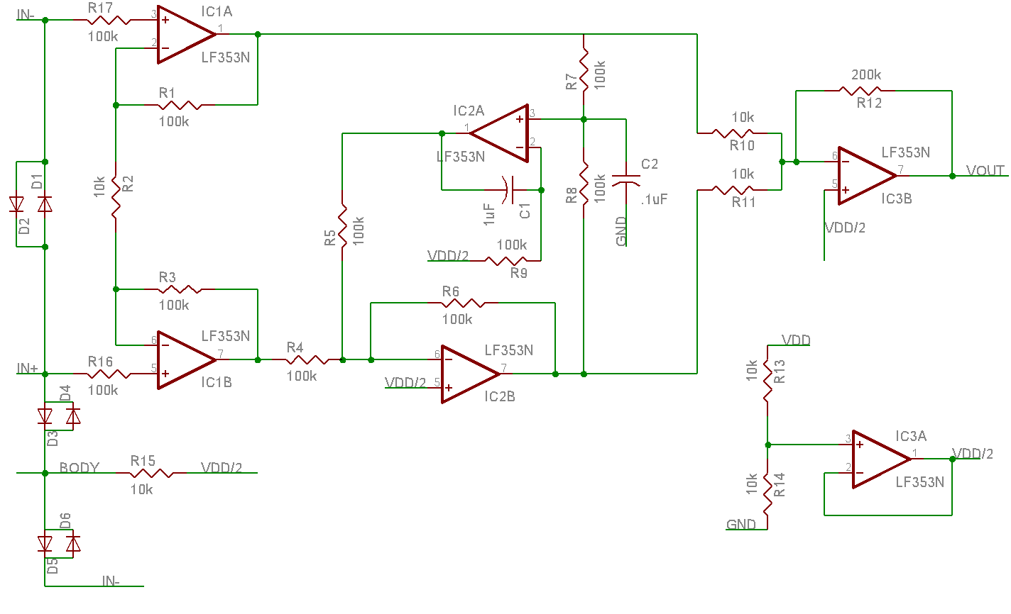
Before I could even start looking for hardware, I had to find a decent schematic. Some google searching about the subject of “DIY EKGs” yielded a good number of websites. The creator of this site, John Nguyen, was generous enough to document his entire process of constructing an EKG from his own original schematic (seen below). Additionally, his design incorporated some neat analog filtering. And thus, Having already attended to the goals of designing an EKG that 1) works with a computer and 2) involves some kind of analog filter, Nguyen’s site naturally became the “textbook” behind this project.

Schematic

John Nguyen’s schematic for the EKG circuit (src: http://www.eng.utah.edu/~jnguyen/ecg/long_story_3.htm)

Several opamp configurations can be seen here:

  • IC3A: Ad buffer that creates a virtual ground at 4.5V for the circuit.
  • IC1A and IC1B: The combination of these two form an instrumentation amplifier with a gain around 20. Its purpose is to selectively amplify the voltage difference between the chest electrodes.
  • IC2B and IC3B: Summing amplifiers.
  • IC3A: An integrator. The exact effect of the incorporated feedback was a bit difficult to isolate. It turns out that this bit of the circuit is better understood at the final summing amplifier (IC3B) where one can see that the integrator works to have the two signal’s cancel each other out if the input ever happens to go stagnate. Imagine the voltage across an inductor when you give it a pulse train for an input signal. This circuit as a whole behaves in a nearly identical manner. This could serve to eliminate any sort of DC bias that may exist across the skin somewhere.

Most EKGs nowadays are designed with a 12-lead configuration. This is not one of them. Rather, this circuit represents just one of those leads.

3) Software

The good thing about software is that I can start prototyping right away. I had at least 50% of the program coded by the day I ordered parts from Mouser. This encompassed a simulator of sorts that would allow me to simulate the electrical waveform of a typical heart beat. Below is a video of the simulator that I used before I was able to collect real heart data. In retrospect, I should have went over everything a bit more slowly, but the gist is that the program has some sliders and things to change what the (simulated) EKG signal looks like, and how it’s displayed to the user.

EKG Software Features from Josh Smith on Vimeo.

More of the program was written after the hardware had been constructed (See section #4) but it’s best to describe the details about how it works right here. The language that I used to create this program was Pure Data. While Pure Data is a visual language typically used for electronic music synthesis, I figured that it had all of the right tools to build the application that I had in mind. With the input being the computer’s audio port, the program takes the input signal and runs it through a notch filter to cut out the remaining 60Hz noise from the mains. From there, peak detection is performed by recording the time when the level of the signal surpasses a specified threshold value. This works only because the R portion of the wave usually forms the maximum amplitude of the EKG signal… for healthy hearts at least. Pure Data has a built in object for this sort of thing called [env~].

The program source code can be downloaded here. Note that the link is a download for a zip file. You also need to download and install Pure Data (official site here) in order to run the program. Once you unzip the file, open WORKSPACE.pd to start playing around.

4) Hardware Construction

All of the electrical components were soldered onto single-sided perf board.

Excluding the cost of shipping the electrical components, I spent $7.26 on this project. While it maybe could have been done for a bit cheaper, I suppose it’s not a bad price when DIY kits of similar complexity may cost at least $20. A small breakdown of my costs is shown below:

Item Cost
Electrical Components $1.76
Tin of Altoids $2.00
RadioShack Perf Board $2.50
9V Battery $1.00
Shipping costs, 1
potentiometer, wire,
Soldering Iron, and
Solder
Free/
Excluded

From here, there’s not much to it except following the schematic, and there are many ways to do this.  I took the freedom to add a 1Mohm potentiometer in series with R12 so that I could have some control over the output gain. Given the chance to do it again, I would give the layout another thought in order to reduce the number of jumper wires I had to use.

5) Testing

Having soldered on all of the hardware, it was time to see how it would connect to the program. The clip below offers a good idea of what the system looks like:

The schematic below shows how I connected the EKG circuit to the computer. Note how R1 and R2 form a voltage divider that brings a 9V signal down to 1V at the computer input.

One thing to be wary about regarding this schematic: saying that the EKG signal spans from 4.5V to -4.5V is not totally accurate, at least for me. During my use, I used the battery’s negative terminal for ground instead of a virtual ground of some kind. This caused the EKG signal to span from 0V to 9V with the baseline sitting at 4.5V. However, the audio input behaves as though it uses a coupling capacitor to eliminate DC offset, so it’s acceptable assume that the EKG signal centers itself at 0V for the sake of focusing upon the amplitude of the signal.

Now to show off some recorded EKG data:

The electrodes were attached in a Lead I configuration (Positive electrode on left pec, negative electrode on right pec). I was bit surprised by how clearly things managed to turn out. The high signal to noise ratio can be attributed to the use of an instrumentation amplifier and a digital stop band at 60 Hz. And, I’ll say this again, It’s important to keep the computer disconnected from mains at all times while recording with this EKG! 

6) Closing Remark

There’s no doubt that collecting clean biological signals poses a good deal of fun. This circuit should see another programming application in the near future.

Extras

Heres a case where the leads weren’t pressed tightly to the skin and the notch filter wasn’t turned on.